
Custom RFID antenna frequency and impedance matching starts with a defined operating band, source or chip impedance, measurement reference plane, bandwidth, enclosure, cable, and target materials. Optimize the radiator and matching network as one system, then verify feed match and radiation behavior across production tolerances and realistic installation states.
“Matched at the center frequency” is not a complete acceptance criterion. The antenna may need useful bandwidth across regional channels, temperature, material loading, bends, or housing variation. A good port match also does not guarantee high radiation efficiency or the required read zone. Matching should therefore be accepted only after the production-intent materials, enclosure, feed structure, tolerances, and installed application have been verified.
Define the reader or chip impedance interface
Reader antennas commonly interface to a nominal transmission-line impedance, while passive RFID tag antennas are designed around the complex impedance of a specific chip. In either case, state the source, load, and reference plane before discussing matching. Include connector, cable, launch, fixture, balun, or probe effects that sit between the instrument and the antenna.
The Keysight Impedance Measurement Handbook provides engineering background on impedance measurement methods, fixture effects, calibration, and frequency-dependent behavior. Use the appropriate method for the impedance range and device structure; a measurement setup intended for a coaxial 50-ohm port may not directly represent a balanced or complex chip interface.
| Comparison Area | Reader Antenna Matching | Passive Tag Antenna Matching |
|---|---|---|
| Target relationship | Match the antenna system to the reader port and transmission-line interface defined by the equipment | Match the antenna input to the frequency-dependent complex chip interface, commonly using a conjugate relationship |
| Source and load | Powered reader RF port, cable, connector, feed, and antenna | Incident RF energy, tag antenna, assembly parasitics, and RFID chip |
| Typical reference plane | Defined coaxial connector, cable end, feed, fixture, or calibrated antenna port | Balanced feed or chip-attachment plane represented through a suitable fixture, probe, model, or assembled-tag method |
| Measurement approach | Calibrated complex reflection measurement, followed by radiation or read-zone verification | Impedance or model correlation plus chip activation and backscatter verification on representative tagged items |
| Fixture dependency | Cable, adapter, launch, balun, mounting, ground, enclosure, and de-embedding boundary | Probe or fixture parasitics, chip attachment, strap, adhesive, substrate, host material, and assembly geometry |
| Acceptance criteria | Required band, return loss or VSWR where appropriate, power handling, pattern, polarization, and installed coverage | Power-transfer requirement over the intended band plus activation, backscatter, orientation, and attached-item performance |
| Installed-state validation | Reader settings, cable loss, mounting, enclosure, nearby structures, tags, and unwanted-read zones | Final chip, antenna, adhesive, protection, product material, bend, orientation, and environmental states |
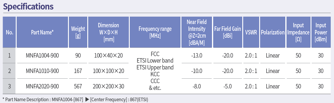
The table preserves an important boundary: 50 ohms is common for many reader ports and laboratory transmission-line systems, but it is not always the antenna target. The target and acceptance method must follow the actual source, load, and reference plane.
Set frequency and bandwidth criteria
For passive UHF RFID, define the regional channels within the GS1 EPC UHF Gen2 protocol range. State whether the matching requirement applies in free space, on a tagged product, inside an enclosure, or across several material states.
The specification should state:
target frequency range and regional variants
source or chip impedance versus frequency
allowed return loss, VSWR, or power-transfer criterion
reference plane, fixture, calibration, and de-embedding method
enclosure, ground, cable, adhesive, bend, and material states
temperature and production tolerances
Choose tuning elements with loss and tolerance in mind
Geometry changes, stubs, loops, slots, lumped inductors or capacitors, and matching networks can move the impedance toward the target. Each option affects bandwidth, loss, current distribution, cost, repeatability, and adjustment access. Select components with realistic Q, tolerance, temperature coefficient, package parasitics, and mounting variation.
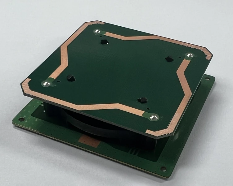
Avoid tuning only one sample to a narrow dip. Use simulation sensitivity sweeps and several prototypes to locate dimensions or components that dominate variation. Reserve a controlled tuning strategy for production-intent hardware rather than relying on ad hoc rework.
Verify matching and radiation separately
Calibrate to the agreed reference plane and retain the complex measurement data. Then verify the antenna’s radiation properties and application performance. A low reflected-power reading can also occur in a lossy structure, so feed match alone is insufficient. IEEE 149-2021 provides the antenna-measurement framework.
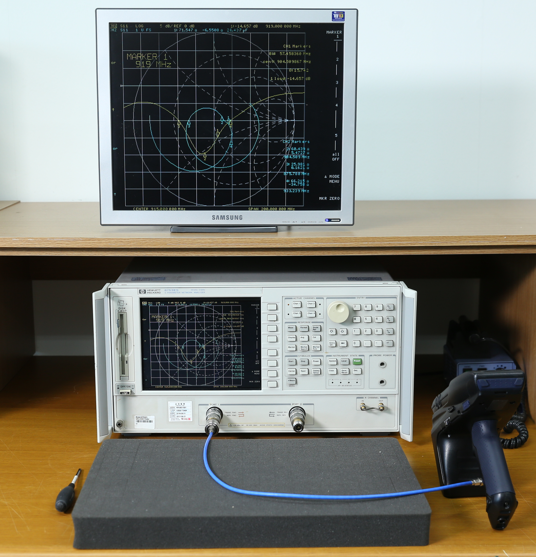
For tag antennas, verify activation and backscatter behavior on representative products and orientations. For reader antennas, verify coverage, polarization, cable loss, and unwanted-read zones. Repeat critical tests across material lots, assembly tolerances, temperature states, and any regional variants.
Frequently asked questions
Is 50 ohms always the antenna target? No. It is common for reader ports and test systems, while tag chips often present a frequency-dependent complex impedance that calls for conjugate matching.
Does the lowest VSWR produce the best read range? Not necessarily. Radiation efficiency, pattern, polarization, tag sensitivity, reader settings, and installation also control the link.
When should matching be frozen? After production-intent materials, enclosure, cables, mounting, and representative tolerances have been measured—not on an isolated early prototype.
Continue with RF technology insights, RF antenna and component resources, and the applications hub.
Review custom RFID antenna frequency and impedance matching requirements.
References
Keysight Impedance Measurement Handbook
IEEE 149-2021 — IEEE Recommended Practice for Antenna Measurements
GS1 EPC UHF Gen2 Air Interface Protocol
https://www.keysight.com/us/en/assets/7018-06840/application-notes/5950-3000.pdf
https://standards.ieee.org/ieee/149/6667/
https://www.gs1.org/standards/rfid/uhf-air-interface-protocol
Related reading
Circular vs Linear Polarization in RFID Reader Antennas
Optimizing Antenna Performance Through Impedance Matching
Inside the RF Measurement and Antenna Testing Facilities at MAC technologies Inc.