
Ceramic antenna development is a system-level trade-off between electrical size, bandwidth, radiation loss, material tolerance, geometry, feed design, mounting, and manufacturing repeatability. A higher dielectric constant can shorten the wavelength inside the structure and support miniaturization, but it does not remove the need to control loss, tolerance, and the installed environment.
Relate permittivity to resonant size
Relative permittivity describes how a dielectric material influences the electric field compared with free space. In a practical antenna, the effective permittivity depends on the material and the field distribution around the geometry, metallization, feed, ground, adhesive, and surrounding air or enclosure. The relationship between permittivity and resonant size is therefore useful for design direction, not a complete sizing formula.

Material values should be tied to a source, frequency, temperature, and tolerance. A nominal catalog value may not represent the exact production lot or the effective value seen by a particular antenna structure. When correlation matters, keep the material record linked to the simulated and measured sample.
Miniaturization creates bandwidth and loss trade-offs
Reducing antenna size often increases sensitivity to loss and tolerance. Dielectric loss converts part of the RF energy to heat, while conductor and interface losses add to the total. A compact resonant structure may also provide narrower usable bandwidth, making material and dimensional variation more visible at the band edges.
The design target should therefore include more than a center frequency. Define usable bandwidth, feed match, radiation metric, polarization, efficiency or gain requirement when applicable, installation state, and expected manufacturing variation. Do not use an excellent return-loss point as the only evidence of antenna performance.
| Design variable | Engineering effect to review | Evidence to retain |
|---|---|---|
| Permittivity | electrical size and resonance | material value, frequency, tolerance |
| Dielectric loss | efficiency and thermal behavior | material data and measured correlation |
| Geometry | resonance, coupling, polarization | controlled drawing and inspection |
| Feed and ground | impedance and current distribution | layout revision and S-parameters |
Geometry and metallization are electrical parameters
Ceramic dimensions, slots, electrodes, vias, edge features, and metallization thickness can all affect the resonant response. The drawing should identify critical dimensions and datums rather than leaving them as uncontrolled manufacturing details. Surface finish, conductor adhesion, and any trimming or tuning process should be linked to the released configuration.
Vary the dimensions and material properties expected to change in production. Use the resulting sensitivity to identify features that need tighter tolerances or additional inspection, and check those predictions against representative builds.
Design the feed, ground, and matching network together
The antenna feed may use a pad, pin, microstrip, coaxial transition, coupling element, or another interface. Its position and geometry interact with the ceramic body and ground arrangement. PCB ground size, clearance, connector launch, matching components, and the route to the radio can change the measured impedance.
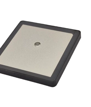
Matching should be performed at a stated reference plane with the intended ground and integration state. Components can help compensate for a measured impedance, but they also introduce tolerance, parasitic behavior, and loss. A geometry or feed correction may be more robust when the mismatch originates in the antenna structure.
Include adhesive, enclosure, and nearby materials
Adhesive thickness and dielectric properties can shift the response, especially when the ceramic element is bonded close to a ground or housing. Plastic walls, coatings, brackets, batteries, displays, cables, and nearby metal also change the effective environment. These items should appear in the simulation or be introduced during production-intent validation.
If multiple mounting states are allowed, define each approved state or a bounded rule. A ceramic antenna measured on an evaluation fixture should not be assumed to behave identically in the final product.
Correlate simulation and measurement
Use controlled drawings, material records, and assembly photographs to make the simulated and measured configurations comparable. For feed measurements, record calibration, reference plane, fixture, cable, and sample identity. For radiation measurements, document orientation, mounting, cable treatment, environment, and processing. IEEE Standard 149 provides antenna measurement-practice context without supplying a project-specific acceptance criterion.
When a frequency shift or loss difference appears, review material values, dimensions, metallization, feed position, adhesive, ground, enclosure, cable, and measurement setup before retuning. Correlation across more than one sample is more useful than fitting a model to a single unit.
Define the production release controls
A ceramic antenna development release package should identify the ceramic material and tolerance, controlled geometry, metallization, feed, ground, adhesive, matching network, mounting condition, inspection points, and RF test. Define change triggers for material formulation, supplier, dimensions, metallization, adhesive, PCB, enclosure, connector, or assembly process.
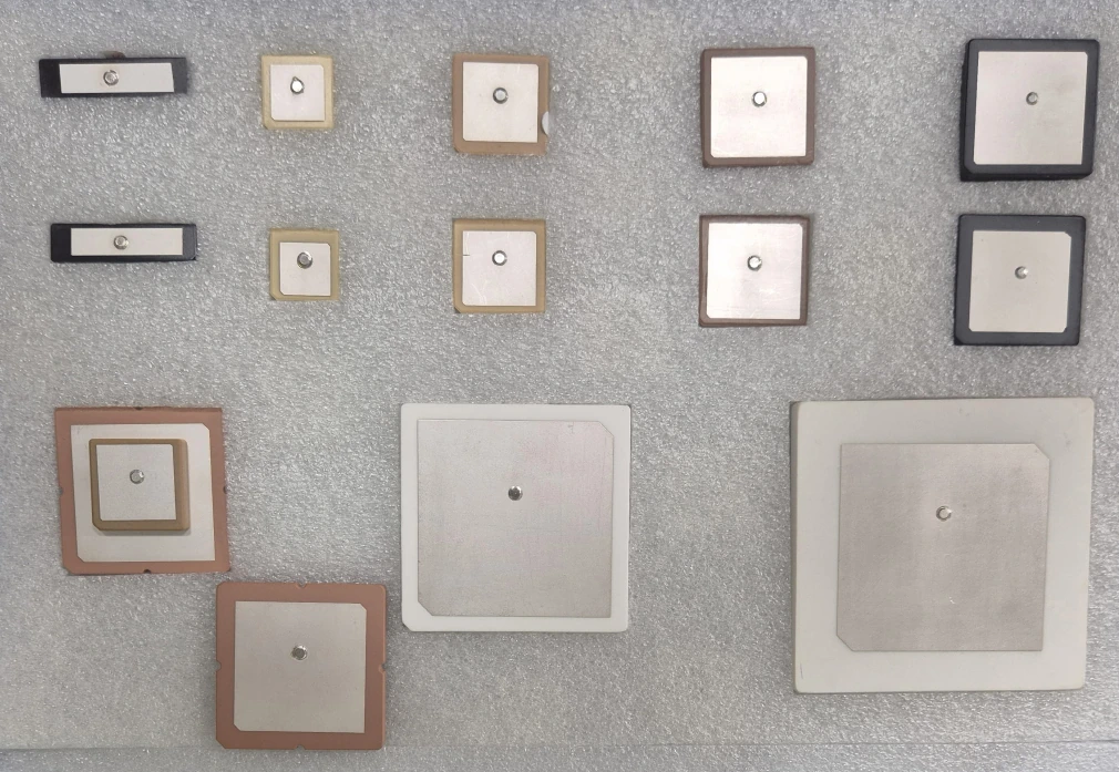
For a ceramic antenna development discussion with MAC technologies Inc., provide the operating band, mechanical envelope, ground and feed boundary, material constraints, installation state, required radiation behavior, environmental assumptions, and validation method. See the applications hub and RF technology insights for related integration guidance.
References
IEEE Standard 149
https://standards.ieee.org/ieee/149/6667/
Related reading
RFID Antenna Design Technologies for Compact Readers
Why Lightweight and Ultra-Lightweight RFID Antennas Matter
Understanding RFID Antenna Characteristics: How to Read a Datasheet